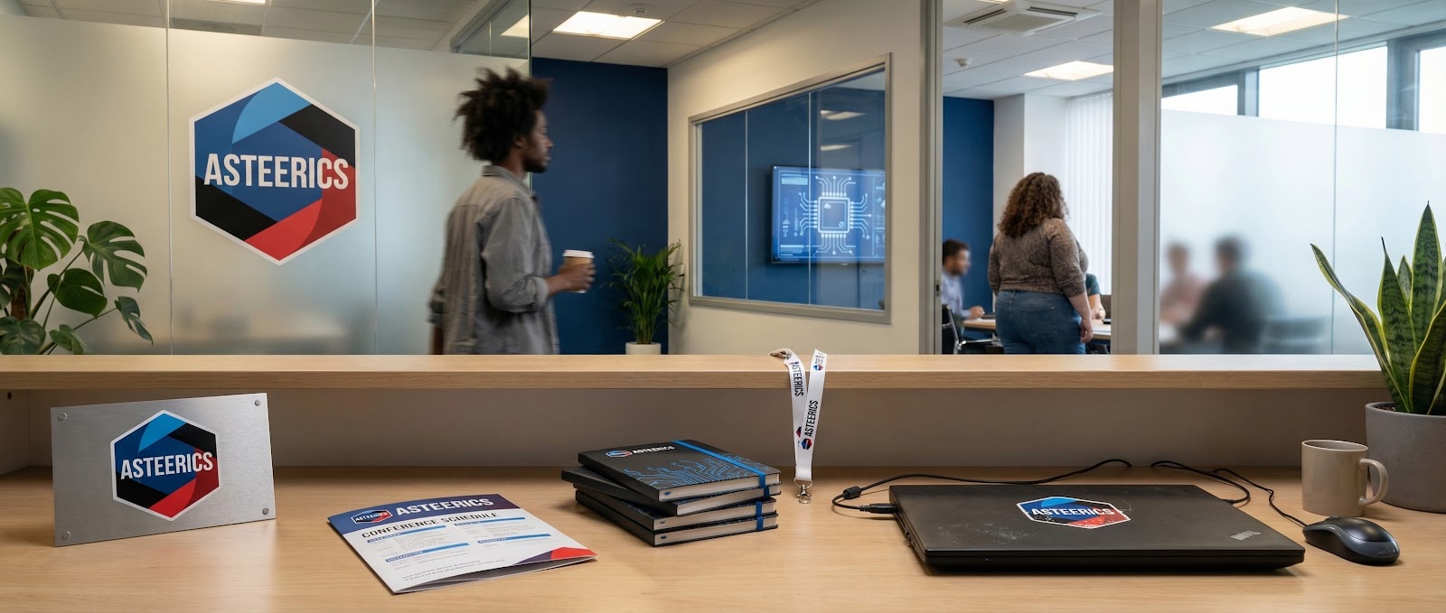
France has launched ASTEERICS, a national microelectronics competence center designed to boost European semiconductor independence under the EU Chips Act. The facility, led by the Minalogic competitiveness cluster, provides chip design tools, prototyping technologies, and foundry access to help European startups and SMEs bring semiconductor concepts to industrial production.
The initiative brings together six major French electronics clusters including Alpha RLH, Images & Réseaux, SCS, Pole via S2E2, and Cap’tronic, creating a unified national network that will operate as a one-stop-shop for the microelectronics ecosystem, according to the aCCCess Network. The center receives co-financing from the European Union through the Digital Europe Programme’s Chips Joint Undertaking under Grant Agreement No 101217840.
As the official French component of the pan-European network of Chips Competence Centers, ASTEERICS will coordinate its efforts through the aCCCess network to ensure alignment with broader European semiconductor strategies. The Paris launch marks a critical step in France’s industrial alignment with EU-wide objectives for chip sovereignty.
Advanced Technologies and Services
The center will focus on three strategic semiconductor technologies: FD-SOI (Fully Depleted Silicon on Insulator), Gallium Nitride (GaN), and Silicon Carbide (SiC), as reported by IT SOCIAL. These technologies are essential for developing high-performance, energy-efficient chips serving critical sectors including AI, IoT, automotive, and power management.
ASTEERICS will provide access to typically cost-prohibitive Electronic Design Automation (EDA) tools and intellectual property blocks that startups struggle to afford independently. The center will also facilitate connections between SMEs and industrial-scale manufacturing, including streamlined access to new European pilot production lines funded by the Chips Act, such as the FD-SOI line managed by French research institute CEA-Leti.
Beyond technical resources, the initiative offers comprehensive business support including training, skills development, and assistance with market launch strategies. The services specifically target fabless startups planning to develop ASICs, ASSPs, FPGAs, or Photonic Integrated Circuits.
Market Impact and Timeline
While the official launch event is scheduled for January 28, 2026, the center has not yet announced specific French fabless startups as initial partners or released quantitative targets for job creation, investment, or production volumes. Industry observers note that these collaborations appear to be still under development.
The initiative represents a significant bet on France’s ability to compete in the global semiconductor race by lowering barriers to entry for smaller companies in the capital-intensive chip industry. Success will ultimately depend on the center’s ability to translate its comprehensive service offerings into commercial victories for European startups competing against established Asian and American semiconductor giants.
Sources
- aCCCess Network
- IT SOCIAL